ECEN 248 Sequential Logic Review
For a pdf version of this review, click here
This review is not all inclusive. I wrote it for the final, which was completely focused on the second half of the class discussing sequential logic. Because of this, topics such as boolean algebra / functions, and combinational circuits are not discussed here. I got a good grade on the final, and this was pretty much the only way I studied, so I think it’s okay for what it does cover.
Topics Covered
- Sequential Logic Design
- Finite State Machines
- RTL Design
- Timing and Optimization
- Sequential Hardware Design
Sequential Hardware Topics
- Registers, Shifters, and Counters
- Memory Types (Register File, SRAM, DRAM, ROM)
Sequential Design
Finite State Machines (FSM)
In sequential circuits, we need a method for capturing behavior and designing a corresponding circuit like we did with truth tables and boolean logic for combinational circuits. It’s slightly trickier here, however, because outputs are based on path as well as inputs, so we need to make sure in our new design system we keep track of everything.
For this, we use what are called Finite State Machines. Breaking down that name we get a good description of what it is:
- Finite: A limited amount of something
- State: In sequential circuits, a state is a place in logic that our circuit can be in
- Machine: A thing consisting of related, interconnected parts, where each part has it’s own function
So putting it all together, we can deduce that the thing we’re building towards is a description of a circuit by breaking it down into a limited amount of connected parts, known as “states”.
But how do we do this?
Well the first step would be to define the basics of the circuit:
- The set of inputs to the circuit
- The set of outputs to the circuit
- The set of states the circuit can be in
From there, we want to give more context to each of those and define the transitions between the states for every input combination. States can loop back on themselves, so if for a certain combination you should stay, just loop back.
Now that we have each state, and the transitions between them, we want to define the behavior of each state, that is, the output that happens when we’re at that state. Only mention anything that isn’t 0, as there is an implicit convention that unmentioned variables are just equal to zero. Once you’ve done all of this, you’ll end up with something that looks like this:
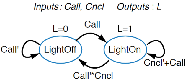
What’s important to note, however, is that there are two different kinds of FSM’s, and the difference between them is simple but very important. What we just described and output is a Moore Machine. The output of these FSM’s is entirely dependent on their state. If you are at state “LightOFf” the only option for output is “L=0”.
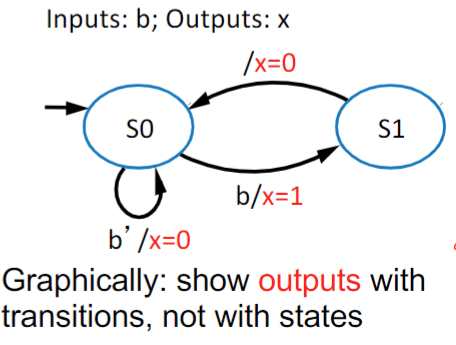
The other kind of machine is what’s known as a Mealy Machine, where at least some of the output is based on the current input as well as the current state. To denote this, we put those outputs on the transition arrows on the FSM like below
Checking Transitions
As mentioned in the design section, you need to make transitions exist for every input combination. Past this, however, you also need to make sure your transitions are Exclusive (No two states could ever be true at once) and Complete (Every possible input combination has a transition).
To check exclusivity of a state’s transitions, you want to take all of the transition conditions, and AND them together. If they are exclusive, when you reduce this term it will come out to be a flat 0, and this means that no two transitions can be true at once.
To check completeness, take all of the transition conditions, and OR them together. If your conditions are complete, then reducing this term will result in a plain flat 1, without any variables. This means that given any condition, at least something will be true.
State Reduction
Suppose you’re given some arbitrary FSM, and it’s very large. There aren’t many inputs and outputs though so it’s likely some of these states are equivalent, so the question becomes, how do you check that and how would you make the FSM smaller? Well, any spot in an FSM has a specific output and points to a variety of different places. I hope then, it’s not too big a jump in logic to say that two states can be deemed equivalent if:
- They have the same output
- For every input combination, they go to the same place
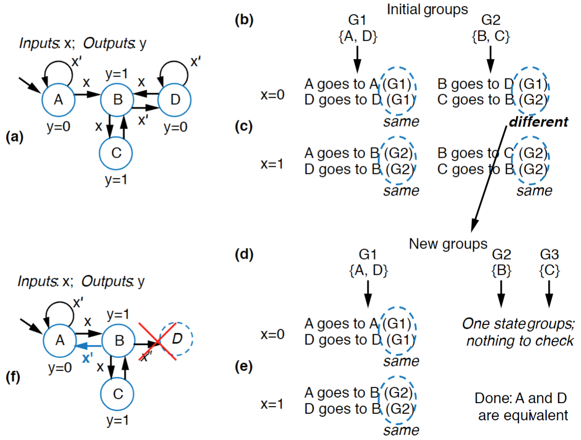
Knowing this, we are given what’s known as the partitioning method for reducing FSM states. It is an iterative process that can feel weird to begin with, but hopefully isn’t too complex:
- Group all of your states together by their outputs to form the top of the table
- Use each input combination as the vertical part of the column
- Inside each cell, for every state in the group, list what group it points to
- If anywhere in the column, two states don’t point to the same group, partition them into different groups and repeat step 3
- Once everything is either a state in its own group or a group of states that completely point to the same thing you have reached your final form
- Any groups with multiple states can become just one state
Controller Design
The last major things to do with FSM’s is to turn them into an actual circuit, which at its lowest level, is made of combinational components and is called a “Controller”. The general structure like of these circuits looks like this:
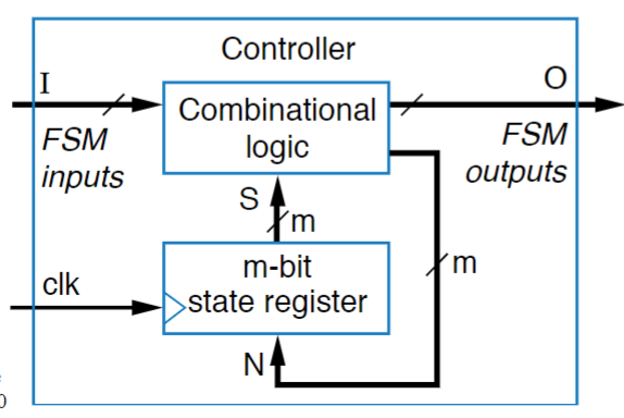
Breaking down the diagram, the “m-bit state register” is a register that we use to store the state of our device. The “combinational logic” is the logic of the FSM, taking in inputs, transitioning to the next state, giving outputs, etc. The wires labeled N cary the “Next State” and “Current State” bits, which are pretty important, but to talk more about that, we have to talk about encoding.
In order to represent our FSM’s with electronics, the first step is that we have to “encode” our states into bits so that the register can actually store and use them. There are many, many ways to do this, but the major ones are below:
- Minimum Bit-width Binary: Assign states in increasing order simply by counting in binary, using as few bits as possible. The first 4 states would
be: 00, 01, 10, 11
- Grey Code: State assignment follows the grey code of only changing one bit at a time need. The first 4 states here would be: 00, 01, 11, 10
- One-Hot: Instead of counting, you assign it to where only one bit is high (“hot”) for each state. The first 4 states would be: 0001, 0010, 0100, 1000
- Output Encoding: This is the most unique of the options, where the states are encoded by their outputs, but this only works if every state has a unique output, otherwise you’re going to end up with duplicate encodings, creating chaos
The tradeoff between the two systems, is that you’ll find your combinational logic to be much much simpler with one-hot, but your register bit-width has to be significantly larger to account for the constraint. You have to have N bits in your register for one-hot, whereas you only need $log_2(N)$ bits for Binary encoding. So in summary, if you have the transistors / space to spare on a larger register, one-hot is the way to go, if your design is very constrained, you want to use Binary.
But, regardless of what system you choose, the next step after encoding is to choose a register that can account for that number of bits, which should be fairly easy in either case. Once that’s done, we have the first major component of our controller finished (the state register) and now we need to do the combinational logic portion.
What’s important to remember moving forward is that we’re designing the logic portion that talks to the register and to the outside world, so as you can see in our diagram, it has more inputs than the FSM originally does, because at any point in time, since it’s a combinational circuit, it has no idea what state the whole controller is in. But anyway, to do this we’re going to fill in a truth table, which will have 4 types of bits on it. The first set of bits are the ones describing the state being input. They’re the one saying “Hey, we’re currently in this state” and they come from the state register. The next set of bits are the inputs to the FSM, it’s what we recognized as an input in our diagram, and they go to the outside world. These first two sets are the “Inputs” to our combinational circuit, and on the other side of the table, we’re going to have the set of bits describing what state to go to, which get fed as the next data to the state-register, and finally we have the output bits that were recognized as outputs on the FSM diagram and can be seen by the outside world.
Once we have all of these things we can fill in our truth table, which in the end looks like this:
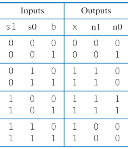
With that truth table, we can find the equations for each output and implement it using boolean logic.
The steps for all of this is below:
- Create the FSM if you haven’t done so already
- Encode your states
- Choose a properly sized register
- Setup and Fill in the truth table
- Design and implement the circuit
Register Transfer Level (RTL) Design
High Level State Machines (HLSM)
So, in the previous portion, we talked about FSM’s, and they were great, but with the tools they had… they weren’t very scalable. For designing incredibly simple circuits, they were great, but, if we need to do more complex things like add two numbers together or store a bit internally, FSM’s just couldn’t handle it. By expanding the capabilities of our FSM, however, to abstract the basics away, we can end up with a much more robust, higher-level design, and we call it a High Level State Machine (HLSM)
These are essentially FSM’s with some extra expansions:
- Multi-Bit Input
- Local Storage (Data that persists between cycles, but the outside world can’t see)
- Arithmetic Operations
In our diagrams, we have a few key conventions to pay attention to here:
- To represent a single bit, wrap it in single quotes (‘’)
- To represent multiple bits, wrap them in double quotes (“”)
- To check equality use double-equals (==)
- To assign a value, use the walrus operator (:=)
- To add a comment use a double backslash (//)
An example HLSM is using all of these is below:
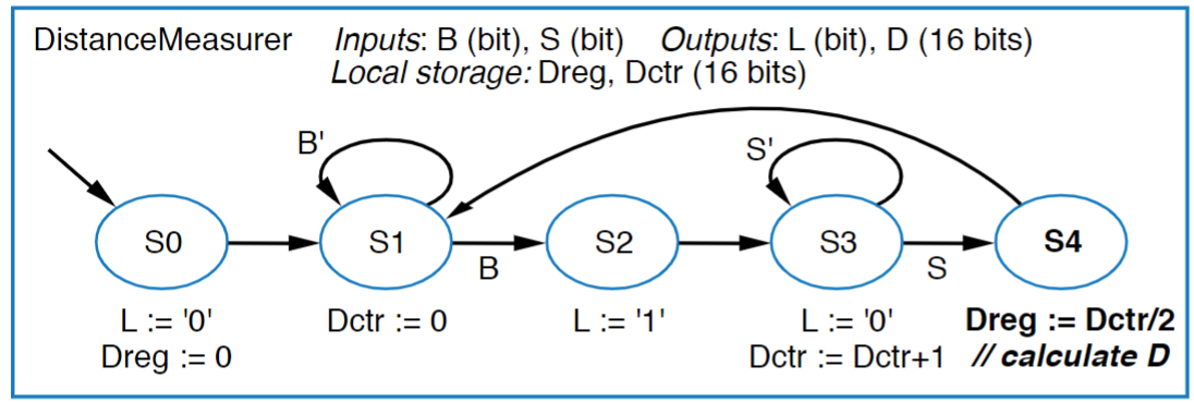
A very important note about HLSM behavior, however, is that changes to stored data happens on clock edges only, whereas conditions are checked anytime. Another way to think about this is that, everything in an HLSM is like a Mealy machine in that it happens on outgoing transitions, so when you’re getting to a state for the first time, it’s data that is checked by conditions on the next cycle is not what it says on the state, it’s one cycle behind, it’s the data that existed from the previous operation.
RTL Circuit
Okay, so once we have a HLSM, turning it into a circuit gets… interesting. Our goal is to turn the high level diagram into two sub-circuits: A FSM backed controller like we saw in the FSM section to control the data, and a Datapath to actually store, alter, and manage the data. The first (and probably hardest) step to complete is to creating the datapath. As a general rule, anything on the HLSM that talks to local storage is on the datapath altered, and on the final controller. So to create the datapath:
- Create a register for every internal storage on the HLSM
- Expose the clear pin of each for assignment to 0
- Use Adders and Shift arithmetic to perform any kind of operation that exists, linking data together to be loaded in
- If you have multiple operations for a given data item, use a mux to select between them
- Expose the load and any mux pins to be accessible to be able to change multi-bit data with single bits.
If you did all of this right, you might end up with something that looks like this:
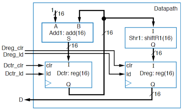
In this diagram, we expose the “Dreg_clr” and “Dctr_clr” pins to be able to assign them to 0, and if you trace the data lines, any time you set “Dreg_ld” to high, It assigns it to the value from the Dctr register shifted right by 1, which is equivalent to dividing it by 2.
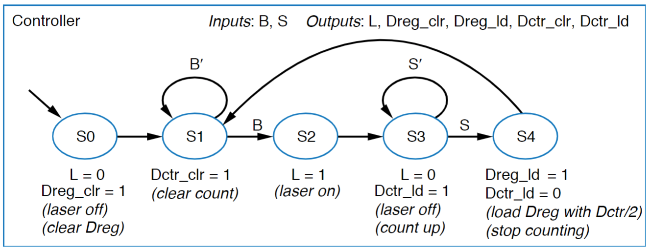
Now that this exists, we need to convert our HLSM to a FSM using the pins exposed from our datapath, which isn’t too hard, since operations have been assigned a specific thing, so it’s just about converting everything to single bit combinations, if you compare the FSM below to the example HLSM, you can see the similarity
Timing And Optimization
Given everything up to this point, we now have a pretty solid basis for building a circuit, but how do we time it? That is, how do we give it a clock that is as fast as possible (so our computer is quick) without going so fast that no data makes it anywhere? Well, that’s what this is all about
Setup and Hold Time
So, every circuit containing registers that we build has 2 separate, but important, timing constraints, known as the setup and hold times. As a note, the values are based on some very low-level things, so instead of calculating them, we are given them on the exam. The Setup Time is the minimum time a signal has to be stable before the clock edge in order for the result to be correct. This stems from the fact that data is stored in flip-flops which are made by 2 flip-flops taking turns with one-another on the clock. If the data changes too close to the clock edge, the correct value won’t be present in the master latch that the slave looks at.
The Hold Time is the minimum time a signal has to be stable after the clock edge in order for the circuit to be correct. This again is due to the fact that flip-flops are made of two alternating latches, and if the signal changes too soon after a clock edge, the signal won’t have had time to propagate completely, and you can create a bad loop inside one of them.
If you violate either of these times by changing your signal too close to a clock edge, you can run into a problem called “Metastability”, where the output of the circuit is not in a set 1 or 0, and it takes time for it to level back out to a set value.
Max Clock Rate
A key concept in avoiding any sort of time violation is to set your clock rate properly. As we discussed in the previous section, the setup time is how long the data needs to be stable before the next clock edge, so if we have a setup time of 1 second and our clock is oscillating at 0.5 seconds, we’re gonna have a problem. Or, on the other hand, if our combinational logic takes 10 seconds to completely propagate, and we’re oscillating faster than that, we’re going to have cycles with bad data in them, so we need to set our clock rate at a speed that ensures everything is done.
To do this, we need to find the Critical Path, which is the longest possible path from any input to register, register to register, or register to output, taking into account any delays. The easy ones to account for is propagation delay and setup time, which sum to give us a easy clock rate. The challenge comes in, however, with hold times, which are conditional. If the propagation delay > the hold time, then you don’t add anything, in the other case, you need to add $(hold time - propagation delay)$ to your time to ensure you don’t violate the hold time.
Once you have your critical delay in seconds (probably to some extremely small power), you can use the formula $f = \frac{1}{T}$ where T is the critical path delay
If this feels weird, it’s important to remember that all of the time violations are with respect to the register storing the data. So we need a clock rate that’s slow enough for the data in a cycle to propagate entirely and safely to the input of the register, but we also have to make sure that our clock is running slow enough that even if we have an insanely fast propagating circuit (like a singular NOT gate), we don’t try and update before the hold time is finished.
Throughput and Latency
When dealing with timed circuits, there are two very important terms to know that give you ways to measure how fast the circuit is running. The Throughput of a circuit is the rate at which data can be input into a circuit, measured in Items per Second. This is closely, closely related to the max clock rate, as by the rules of the max clock rate, you can only input 1 item per clock cycle. As you might guess, to increase our throughput, we’d want to find a way to speed up the clock.
On the other hand, we have Latency, which is the measure of how long it takes new input data to result in new output data, measured in seconds. This is… sort of the critical path. If your circuit only has inputs and then a final result register, it is the critical path. But if you have multiple sets of registers in your circuit (like in the case of pipelining), it is the total longest propagation delay.
Pipelining
Okay, now that we have stuff defined, lets see what we can do to speed up circuits. An easy way to do this is to “break up” your circuit into a series of sequential tasks. The pretty solid example provided in the slides is you can think about it like doing dishes. If you’re doing them by yourself, then it takes a long time because you have to both wash and dry every dish. If you have a friend, however, you can double your speed, because you wash and then hand the clean dish to your friend to dry and put away while your washing the next one. The total time spent handling every dish is the same, but you can wash more in the same amount of time because you work on the different tasks at the same. We call this pipelining because we create a “pipeline” similar to a factory line.
The same logic applies here, if you break up your circuit into a set of steps, and at the end of every step, add an extra register known as a “pipeline register”, you can decrease your critical path, allowing your circuit to run much, much faster.
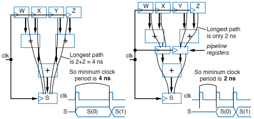
There’s a few things to note of though:
- This affects throughput, in that you can handle more items per second with the faster clock rate, but it does not affect latency, it still takes the same amount of time for one particular data item to get through
- There is a limitation here: A step can’t run faster than the setup or hold times for the registers, otherwise you’re going to create violations.
Concurrency
Continuing with our dishes example, what if, instead of bringing in a friend, we split our dishes into stacks, and then gave them to two other people to wash in separate sinks at the same time as us. We would have a very strange kitchen on our hands, but also, you’d notice that the rate at which you could clean and put away dishes would increase drastically, as it may take 4 seconds to completely clean and put an individual dish away, but now you have 3 people doing it at the same time, which means in a 4 second window, you’ve now cleaned 3 dishes instead of 1, meaning your time to complete the overall task has decreased by a factor of 3! This is called concurrency because you end up with multiple systems working “concurrently” to complete the task faster
The same idea apply’s to circuits. If you have to do say, 256 additions, instead of doing those one after another, you could break them up into groups of 16 and massively speed up your circuit.
Sequential Hardware
Registers
Registers are the simplest device that we frequently work with to store information, but they’re not anything crazy, it’s just a group of D flip-flops sharing a single clock line. N-bit registers can have a width of N, meaning they can store N-bits, with common widths being powers of 2. The simplest register loads its data on every cycle, which is great, for things like keeping track of the state of a circuit, which can change on every cycle, but it’s less great for tasks like counting, where if you loaded an input on every cycle, you’d never be able to start counting, so past the basic register, there’s a few different types.

Parallel-Load Register
This is the kind of register we’ll use for tasks where we don’t want to load data on every cycle, which is applications like counting. To accomplish this, we’ll add two things. The first is an extra input signal to our register called “Load”, often abbreviated to “ld”. The other thing, which is actually a bunch of the same things, is a 2x1 Mux to every bit. With these two things, we can make it to where when Load is high, it reads the data from the input pins, but when load is low, the mux just gives the current output back to the flip-flop. So now, the flip-flop still receives a signal on every clock cycle, it just only updates with external data when load is high. It is called a Parallel-Load register because all of the bits load new data in parallel (at the same time), rather than waiting for anything else to finish.

Shift Register
This kind of register is used for temporary data storage. If you only need to keep a value for a small amount of time, like a thermometer reading a temperature, a shift register can be very useful, although usually it’s in combination with other registers. The simplest one will move data to the right, losing the rightmost point, and adding a zero to the front, and we accomplish this by connecting the flip flops in series rather than in parallel. But this basic configuration isn’t very fun, because it’s impossible to get data in in the first place. The standard shift-register has two additional pins. The first is the “Shift Right” pin, abbreviated to “Shr” controls wether it should actually do a shift, and uses a 2x1 mux like in the parallel-load register. The second is the “shr_in” pin, which is the value to shift in, and can be 0 or 1. Putting this all together, we get the circuit seen in the below figure
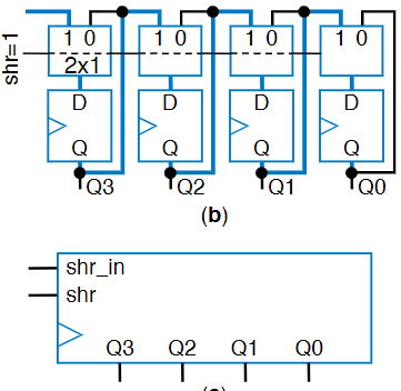
Quick note, another kind of shift register is the rotate register, where instead of having a shr_in pin to pick it’s next number, the rightmost bit that is being shifted out becomes the new leftmost bit.
Multifunction Registers
Each of these can be fun on it’s own, but for each of those features, we have to get a different register, which can be less than ideal if all you need to do is load something and then shift it. Like we saw before, however, mux’s can come in super handy, because all we need to do for a given register is control what data gets given to each flip flop. Building on this, if instead of using 2x1 mux’s, we used Nx1 mux’s, where N is the number of functions we want our register to have…. well, we can start making our one little mux do a lot of different things. Then, we just expose the select bits of the mux as register pins and we can do as much as we want.
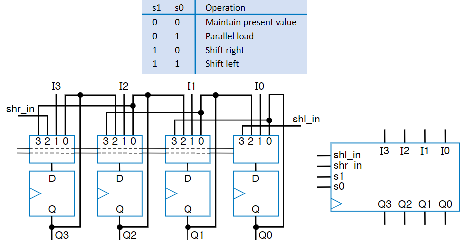
There’s two additional things to note here with multifunction registers. The first is that load typically has the highest priority, and you need to make sure you design your mux such that it doesn’t care about any of the other pins when load is high. The other key thing to note is that given a small number of functions, instead of having to remember the exact combo of the select pins (Knowing 11 is load while 10 is shift left), registers will also often have internal combinational logic to just expose pins that select a function, ordered highest to lowest priority, top to bottom.
The steps to design one of these registers is below:
- Determine the mux size by counting the number of operations (including the maintain present value) and add a mux in of that size
- Create an operation table defining the function you want for each select line option
- Connect the mux inputs to the corresponding input sources based off of your operation table
- Map control lines to expose simplified pins by using a truth table and assigning priorities
Shifters
With a circuit like our shift registers, we can do multiplication and division veery quickly. These circuits are called “Shifters” and they are just function devices, they don’t store any data, they just transform what they are given and spit it back out. It’s basically a box of linked mux’s.
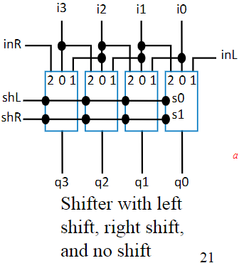
Now the reason these are so powerful is because they make multiplying and dividing by powers of 2 super quick:
- Multiplying: 011(3) Shifted left once becomes 110(6). By appending a zero to the end, you are doing the same thing as you do in base 10,
increasing the magnitude of the number by 1.
- But do note overflow, if you tried to do 110(6) shifted left again, you’d end up with 100(4), not 12. So when doing things, you need to make sure you have sufficient bits to not lose data!
- Dividing: 110(6) Shifted to the right once becomes 011(3). This is just like the multiplying thing but backwards.
- Note, however, that if we did it again 011(3) would become 001(1). We’re not keeping track of decimals here, there is rounding, don’t get messed up.
The simplified symbol for a shifter is below, where N means that you shift your data, N times, causing you to either multiply or divide by $2^N$

To do multiplications by numbers that aren’t powers of 2, we can do a “shift and add” operation. For example, if we want to do $5 * X$, instead of using some big, nasty, multiplier circuit to achieve that, we could rewrite it as $(4*X)+X$, which can be achieved by double left shifter («2) and a single adder, keeping everything to simple.
Division is a bit trickier to split like that, because you have to get your fraction in terms of a base of 2, but you also don’t have an infinite bit-width either, so you’re pretty much always going to end up with an approximation. For example, if you needed to divide by 5:
\[\frac{1}{5} = 0.2 \approx \frac{102}{512} = 0.199\] \[102 = 64 + 32 + 4 + 2\] \[\frac{X}{5} \approx \frac{64X + 32X + 4X + 2X}{512}\]So now that everything is represented in powers of 2, we can use our left and right shifters to multiply and divide respectively. But there’s a problem. Because we had to make an approximation, pretty much every division introduces some amount of error. So when dividing circuits it’s vital that you combine any similar divisions into as few as possible, and division should be held off for as long as possible to keep the error from propagating.
Barrel Shifters
But how do we shift by 2 or 7 or some other arbitrary bit amount? Because the shifter we discussed at the top of this section could only shift by 1 bit at a time, but then to do operations, we frequently have to shift by amounts greater than 1 (because who ever does math only multiplying by 2?). A naive approach would be to just put in a larger mux, specifically Nx1, linking everything together that way. This might work fine for 2 or 3 bits, but then, when we hit the still relatively small size of 8 bits, we’d be in trouble. That would be a completely filled out 8x1 Mux for all 8 bits, leaving us with 64 wires. But that’s only for one direction, if we wanted to shift in both left and right, we’d either need a 16x1 or 8x2 mux, but still it would be completely filled out! That is… very large, with 128 wires, leaving you prone to glitches and things breaking.
What if, instead, we create a shifter that shifts by increasing powers of 2, so for 8 bits you create one that shifts by 1 bit, and then by 2 bits, and then by 4 bits, with the higher powers still containing 2x1 mux’s, the connections just shift that many bits, and then you put them in series with one another. You may be thinking, “Well this is going to shift by 7 bits every time, all you’ve done is create a strange 7-bit shifter” Except you’re wrong. Each of these shifters has an enable pin that decides wether to shift or output the current value, which means, if we expose those 3 pins from each individual shifter, we can create what’s known as a barrel shifter that shifts based on the number of bits it’s told. Do remember, shifting 8 bits is… unnecessary, because then you’d just replace everything.
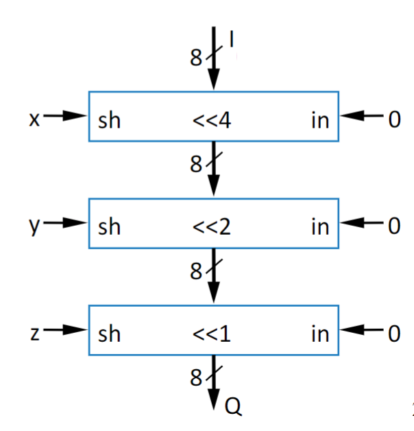
Counters
Now suppose we wanted to do something that we learned to do in approximately the first grade: counting by 1, but being the lazy beings that we are, we want electricity to do it for us. So, like good engineers, we spend far more time figuring out how to do this side project than we ever would have if we just counted in the first place.
So lets describe the counter:
- It starts at 0
- Every time the clock goes high, it increments by one
- It outputs its current value
- Once it has hit it’s highest value, it sets an extra pin to high to let us know.
Given all of this information, we can think think think. A register can store data and only updates on every clock…. A adder can do the incrementing…. An AND gate can check if everything is high… so if we put it all together, we can make a pretty cool little up-counter
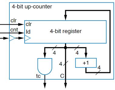
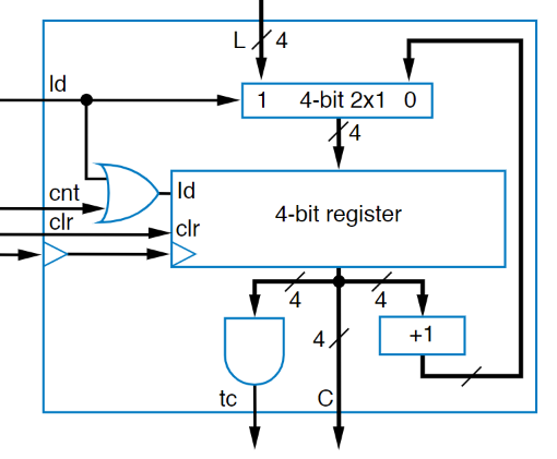
But suppose we want to be able to load in a specific value? So that we don’t have to start at zero. Well, like with pretty much everything else, we use a 2x1 mux to select between the updating the current value or loading another one in:
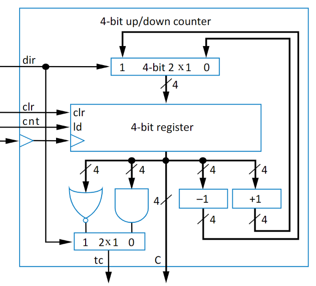
The other individual concept that we could add to the up-counter is to do the opposite, go down. Rather than using a adder, we’ll use a subtractor, and instead of an AND to check that everything is high, we’ll use a NOR to check that everything is low. These changes are below
So what are counters used for? The most common use is making a fast thing… slow.
Clock Division
Like we already talked about, counters count on every clock pulse, so they increment the value at whatever frequency the clock is running at. To this end, that means the LSB oscillates back and forth at $\frac{1}{2}$ of the frequency of the clock, because it is on for one full cycle and off for one full cycle. The bit after that oscillates at $\frac{1}{4}$ the clock rate because it is off for two cycles, once while the LSB is low and once while the LSB is high, and then high for two cycles for the same reason. The next bit oscillates at $\frac{1}{8}$ the clock rate because it is low for the 4 cycles bit 2 needs and then high for another 4 cycles. Do you see the pattern emerging here?
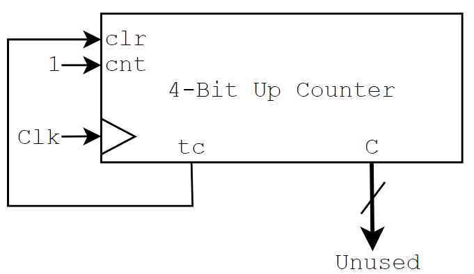
Because of the properties of binary counting, by tracking a certain bit on a counter, you can create a new, slower frequency than the one originally input! This formula generally takes the form $C_{out} = C_{in}*\frac{1}{2^n}$ where n is the bit you’re looking at, with n = 1 for the LSB. If we want to divide our clock by a nice, even power of 2, we could even make our jobs really easy, we could take our output clock to be connected to the terminal count (tc) pin of the counter, and then just make the counter $n$ bits wide.
But now we’re running into a bit of an issue…. We connected our clock to the tc pin, let the thing count, and it set high at the correct amount of time later, but then… the clock stopped. The tc pin is high when we’ve reached our highest value, there’s nowhere else to count, so the progress stopped, but the issue is that we we’re trying to get a clock, not just a delayed high signal. It’s okay though, this is a pretty easy problem to solve, just make a feedback loop so that when the tc pin is high, we link it back to the clear pin (clr) to reset our counter. Putting this all together, we get the circuit below:
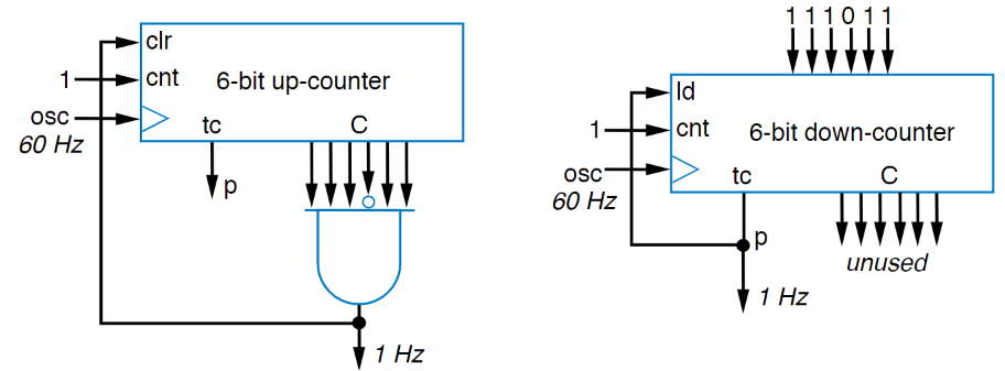
But what if you want to do something wonky, like divide by a number that isn’t a power of 2? Well, that’s not terrible, another way to think about our clock dividers is that their output only becomes high after some number of clock cycles, so if we know the frequency of both the input signal and the output signal using the formula $Count = \frac{C_{in}}{C_{out}}$ then we can find the count we need to be at before signalling our output as high, resetting our counter, and continuing the process. Except…. That’s wrong…. It’s close…. But Definitely wrong.
Here’s why. If we used that count, then our counter would start, on the first clock cycle, at 0, and then count once per cycle until it hit the number we calculated. It’s vitally important that we remember the starting place for a counter is 0 and not 1, otherwise we’d end up with a new clock that is very close to our expected frequency but slightly off. The updated count to do the reset at then becomes: $Count = \frac{C_{in}}{C_{out}} - 1$
Memory
All of the things we’ve been talking about are built for small scale. Storing and accessing a few bits of data is very easy to do directly from a register. With so little data, wires never get crossed, and asking for what you want is a breeze and very fast. But very rarely in computing do we work with just a few bits of data, so to scale our circuits, we need to have a way to easily store and access everything. That is what this section is about.
All of the memory types we’re about to discuss are called MxN Memory, where M is the number of “words” (the number of data slots), and N is the number of bits each “word” has in it. So a 16x8 piece of memory could store 16 different 8-bit values.
Register Files
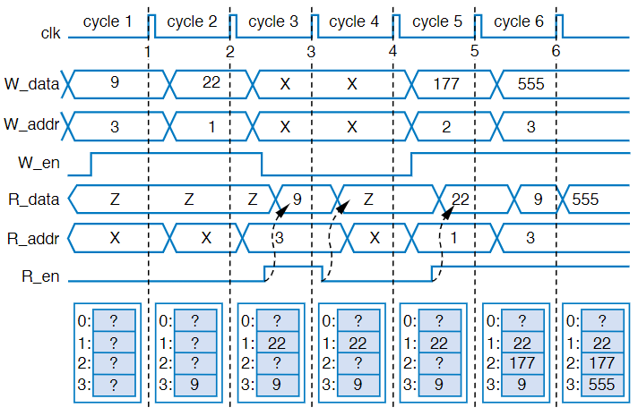
The fastest (and most unique) way to scale storage is through a MxN register file where M is the number of registers and N is the bit-size of each one. These operate by assigning an unique address to each contained registers, and only allowing 1 write operation per cycle, but still allowing reads to happen at any time. This synchronizes all of your writes, preventing race conditions, but still keeps data very accessible, making it really easy to manage data. Great. But how does it work?
I. Don’t. Know. It’s very complex, and quite frankly I find it unlikely for the internal details to be seen on the exam, but that’s the key behavior.

To analyze them, we use a timing diagram like we’ve seen before:
Random Access Memory (RAM)
RAM is memory that you can both read and write to, and it’s pretty similar to a register file. The difference, however, is that it uses storage methods that are much more efficient than registers, so it can store far more words, around 512 to 1024!
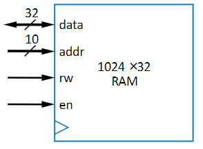
There are 4 pins:
- data: If you’re in read mode, it’s the data pulled from the word, but if you’re in write mode, it’s the data you’re putting into the word
- address (addr): The address of the data you want to access. This is the address of the word, and it connects to a bunch of individual single bit cells
- read-write (rw): The pin deciding if you’re reading or writing to the flash. 0 = Read, 1 = Write
- enable (en): The pin deciding if anything operation will happen. The “on” switch
Inside, it is a decoder with the output connected to each word, and the word has a string of cells connected to it
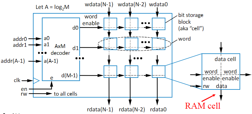
Every cell has a “Word Enable” line coming from the decoder, which tells them that the specific word they belong to is being looked at. The read-write signal is given to every cell individually, but the diagram gets messy so we pass on drawing it.
Static RAM (SRAM)
This is the easier of the two RAM types to understand. It is basically just a NOT gate loop to keep the bit alive with some transistors in place connect it to the outside world. All together it has only 6 transistors (4 being in the form of NOT gates), making it much smaller, than the Register file, while still keeping things very fast. The big idea here is transistors and NOT gates, as the actual function of it is to complex for the course
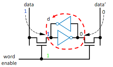
It gets the name “Static” because once the data is in there, as long as the circuit is powered, it doesn’t need to be touched again, so it’s static. This is the big difference between SRAM and the other type we’re about to talk about
Dynamic RAM (DRAM)
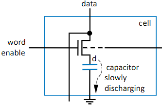
The other kind of RAM is really not that much more complex. Instead of using a bunch of transistors, we instead use a capacitor to store our bit, along with 1 transistor. Because of the simplicity of the circuit, it’s super small, having the smallest footprint of any memory type we’ve talked about, so if you need large storage, this is the way to go. On the other hand, however, it also has some challenges, specifically due to the introduction of a capacitor, as those take time to charge up, making write operations significantly slower. In addition, because it’s in a capacitor connected to ground, the signal will also slowly get lost over time, and has to be refreshed in order for the data to stay good, and that’s where the “Dynamic” part of the name comes from.
Read Only Memory (ROM)
This is the third major memory type, and the most different from the other two in its behavior. The key difference here is that it’s “read-only” (sometimes, we find exceptions). Other major features include the facts that it is faster for reading, lower power, more compact, and the big one: it’s non-volatile, which means that even if the system loses power, it retains its memory. It’s the kind of memory you want if you won’t be changing things very often.
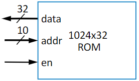
There are multiple kinds of ROM, but I’m going to speed run them. If you want more details, they are in RTL2 slides, starting at slide 13
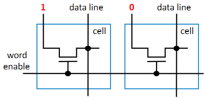
Mask Programmed ROM
Cells get hardwired to 1’s or 0’s at manufacturing to match a certain “mask”
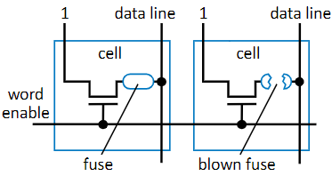
Fuse-Based Programmable ROM
This isn’t programmed by the manufacturer, it uses a special device to program the cells, by overloading them with a high voltage to break a fuse, marking something as 0. It’s also known as One-Time Programmable (OTP) ROM because the consumer can program it one time to suit a specific purpose
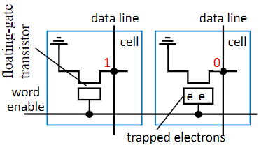
Erasable Programmable ROM (EPROM)
Uses a floating gate transistor in each cell. A special device charges cells marked “0” with a bunch of electrons, trapping them in the gate and pulling the cell low. This is different from the OTP rom because if you shine a UV light onto the chip, it will erase all of the data as the trapped electrons will receive enough energy to escape.
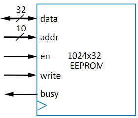
Electronically-Erasable Programmable ROM (EEPROM)
Similar to EPROM, except instead of UV light, we do it with electricity. The tradeoff here is that it’s done one word at a time.
Flash Memory
Similar to EEPROM in that it is in-system programmable and can be edited on the fly, except this one is set up to where large blocks of data can be erased at once.